
Controlled Impedance: Stack-up Design and TDR Verification
Impedance is set by geometry and dielectric, not by the trace alone. How to specify a target that a factory can actually hold, and how TDR coupons prove it.
Specify three things and the factory can hold your impedance: the target value, the tolerance, and the reference layer the trace is measured against. A drawing that says only 50 ohm without a stack-up is a request for an engineering query, not an order.
Impedance is a function of trace width, trace thickness, dielectric height to the reference plane and the dielectric constant of the material. Change any one of them and the impedance moves. This is why impedance control is really stack-up control.
01What moves the number
Dielectric height is the most sensitive variable and the one most often mis-specified. Prepreg thickness is not fixed: it compresses during lamination, and the amount of compression depends on resin content and how much copper is on the layer. A stack-up calculated from nominal prepreg thickness will not match the pressed board.
Copper thickness also varies. A 1 oz specification means roughly 35 micrometres of finished copper, but plating adds thickness unevenly across a panel, and etch-back narrows the trace at the top more than at the base. For tight impedance, give the finished copper weight and let the factory model the etch profile.
- Dielectric height to the reference plane, after lamination, not nominal
- Dielectric constant Dk at your actual signal frequency, not the 1 MHz datasheet value
- Finished copper thickness and the etch profile that goes with it
- Trace width and the spacing to adjacent traces in the same layer
- Solder mask thickness and its Dk, which matters on outer-layer traces
02Single-ended and differential targets
Differential impedance is not twice the single-ended value. It depends on the intra-pair spacing as well as the geometry to the reference plane, and the coupling between the two traces lowers it.
| Single-ended 50 ohm | RF, general high speed signalling. The most common request |
|---|---|
| Single-ended 75 ohm | Video and some telecom interfaces |
| Differential 90 ohm | USB, PCIe at lower data rates, LVDS |
| Differential 100 ohm | Ethernet, USB 3.x, PCIe, HDMI |
| Differential 85 ohm | Some high speed serial links specified by the chipset vendor |
03How to specify it on the drawing
A complete impedance note gives the target, the tolerance, the layer, the reference plane and the structure. For example: 100 ohm differential, plus or minus 10 percent, on layer 3 referenced to layer 2, edge-coupled stripline, with the stack-up as shown.
Tighter than plus or minus 10 percent is achievable but costs more, because it narrows the process window and raises the scrap rate. Plus or minus 7 percent is the tightest we recommend specifying unless the chipset vendor requires it.
04TDR verification
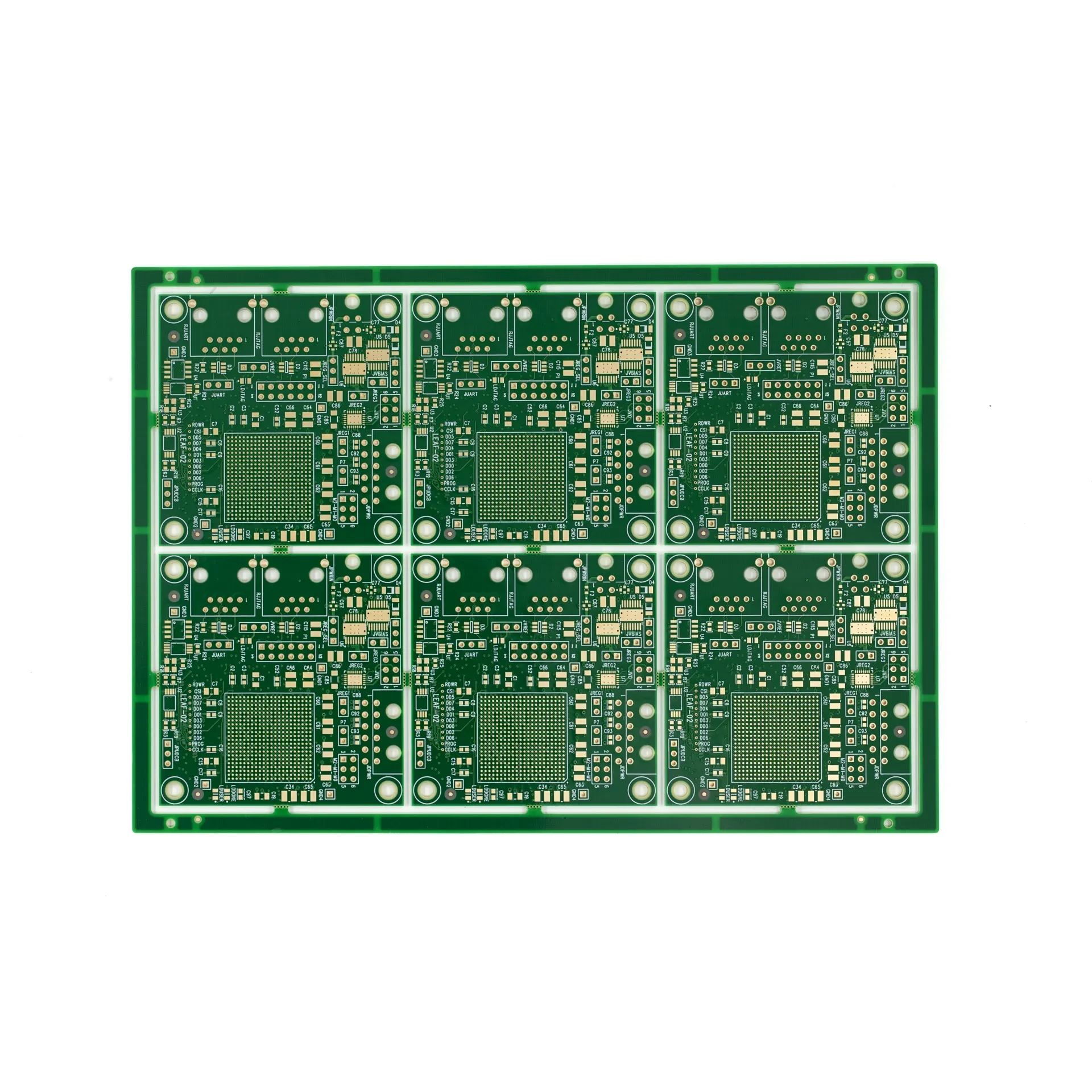
Impedance is verified on a coupon that travels with your board on the same panel, made from the same stack-up and processed in the same run. The coupon carries a trace of known length with the target geometry, and a time domain reflectometer sweeps it to produce an impedance profile.
Ask for the TDR report on the first article of a new build, and for every lot on production runs where the impedance is critical. The report should show the measured value, the target, the tolerance and the coupon identifier so it can be tied back to the lot.
Key takeaway
Give the target, the tolerance, the layer and the reference plane on the drawing, use the Dk value at your real signal frequency, and require a TDR coupon report that is traceable to the lot.
Products discussed in this article
Continue reading

Ready to start your project?
Send your Gerber files for a quote. Simple boards are quoted within 1 hour, complex builds within 24 hours.