
Multilayer PCB
4 to 40 layer boards with controlled impedance for communication, server and industrial designs.
Overview
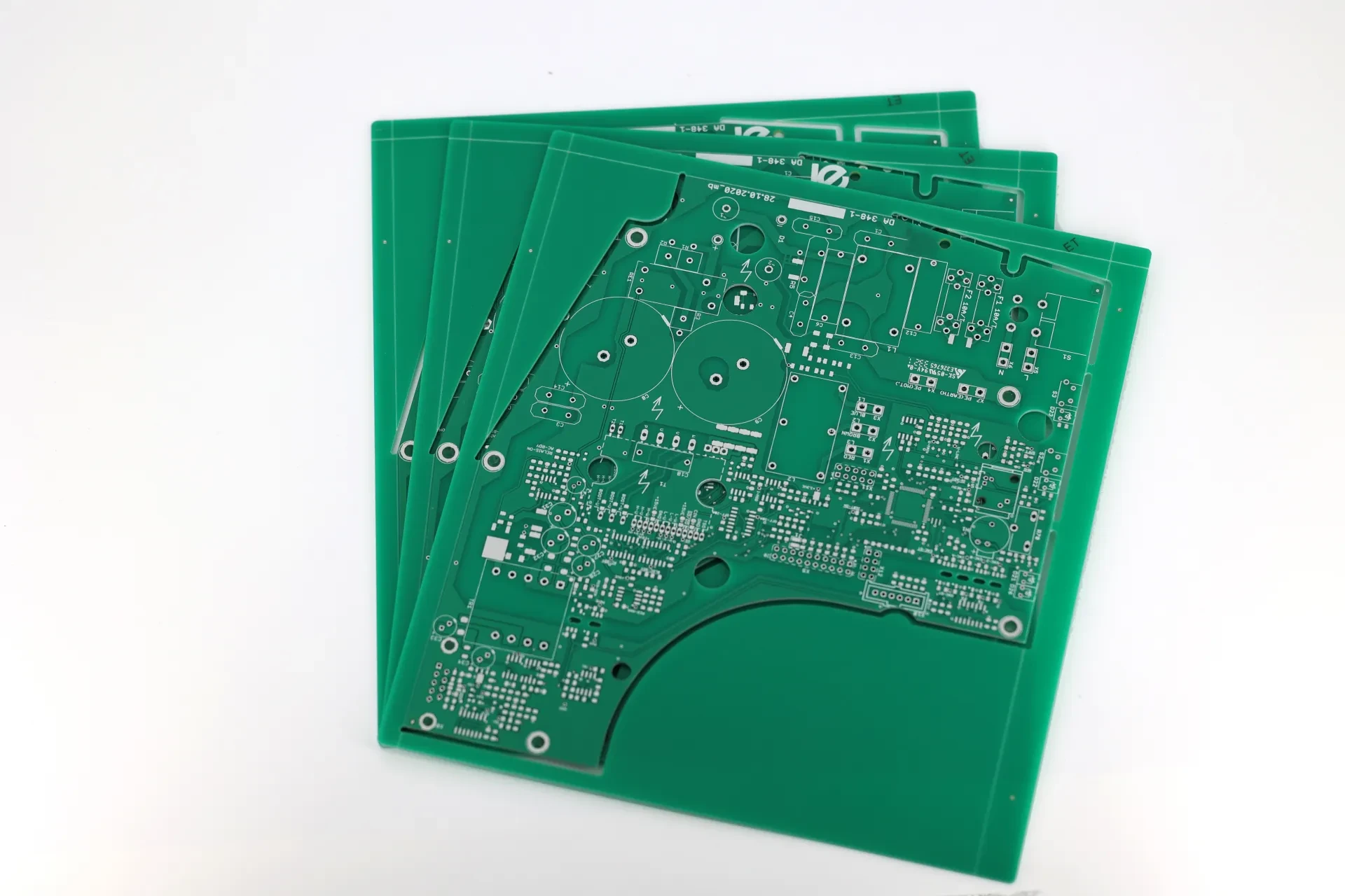
Multilayer PCBs stack copper signal planes and dielectric prepreg into a single laminated board, which keeps high-speed signals short and power distribution stable. Aisler builds 4 to 40 layer boards on FR-4, mid-loss and high-speed laminates, with sequential lamination available for boards that mix buried vias and thick copper sections. Every multilayer order is reviewed for stack-up symmetry, drill-to-copper clearance and press tolerance before it is released to the line.
Key construction features
- Layer count from 4 to 40, with sequential lamination for mixed structures
- Controlled impedance tolerance of ±10% on standard stack-ups
- Buried and blind vias supported alongside through-hole vias
- Inner-layer AOI before lamination, cross-section check on first article
Manufacturing specifications
Standard production capability for multilayer pcb. Tighter limits are confirmed during DFM review.
| Layer count | 4 - 40 layers |
|---|---|
| Board thickness | 0.4 - 6.0 mm |
| Min trace / space | 4 / 4 mil (3 / 3 mil advanced) |
| Min mechanical hole | 0.2 mm |
| Copper weight | 0.5 oz - 6 oz outer, 0.5 oz - 3 oz inner |
| Surface finish | HASL, ENIG, OSP, immersion silver / tin |
| Impedance tolerance | ±10% standard, ±7% on request |
| Lead time | 3 - 15 working days |
Typical applications
- Communication base station and switching equipment
- Servers, storage and data centre hardware
- Industrial controllers and drive units
- Test and measurement instruments
Related products

Ready to start your project?
Send your Gerber files for a quote. Simple boards are quoted within 1 hour, complex builds within 24 hours.