
Advanced PCB
HDI PCB
Microvia and fine-line high density interconnect for compact, high pin-count designs.
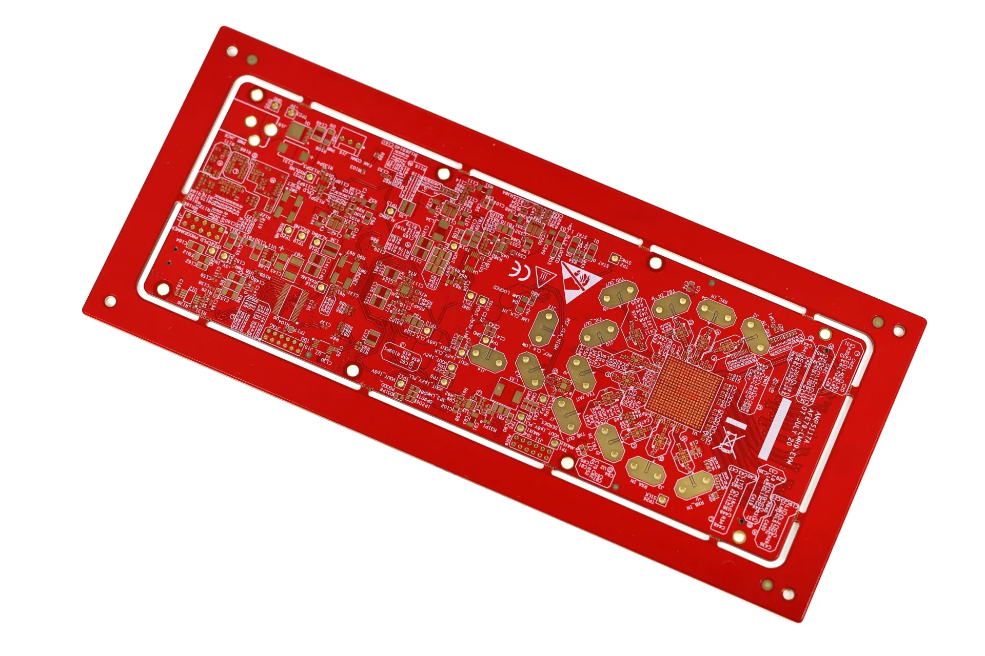
Overview
HDI boards replace mechanical through-holes with laser-drilled microvias so routing can escape dense BGA packages without adding layers. Aisler produces 1+N+1 through 3+N+3 structures with via-in-pad copper plugging, and any-layer interconnect for the most compact designs. Laser via diameter, pad size and stack depth are confirmed against your BGA pitch during DFM review.
Key construction features
- Laser microvia from 0.1 mm, mechanical drill from 0.15 mm
- Via-in-pad with resin plugging and copper capping
- Any-layer HDI and stacked / staggered microvia structures
- Fine-line imaging down to 3 / 3 mil trace and space
Manufacturing specifications
Standard production capability for hdi pcb. Tighter limits are confirmed during DFM review.
| Structure | 1+N+1, 2+N+2, 3+N+3, any-layer |
|---|---|
| Laser via diameter | 0.1 - 0.15 mm |
| Min trace / space | 3 / 3 mil |
| Board thickness | 0.3 - 3.2 mm |
| Surface finish | ENIG, immersion silver, immersion tin |
| Lead time | 5 - 15 working days |
Typical applications
- Smartphones, tablets and wearable devices
- Camera modules and compact sensor boards
- Automotive ADAS and infotainment units
- Portable medical diagnostic devices
Related products
Ready to start your project?
Send your Gerber files for a quote. Simple boards are quoted within 1 hour, complex builds within 24 hours.